This blog post shows how easy it is to create a SOT-23 package transistor with Altium designer IPC Footprint Wizard.
The transistor for which we are going to create the footprint is the MMBT3904LT1G from ON Semiconductor. The picture below shows how it looks like-
If you download the datasheet of this component you will find the dimension of the body and the footprint. The picture below shows the dimension cut from the datasheet-
This engineering drawing has all the dimension we need.
Once you have opened your PCB Library component editor in Altium Designer, click on the IPC Complaint Footprint Wizard which is under the Tools in the toolbar.
The startup window looks like this-
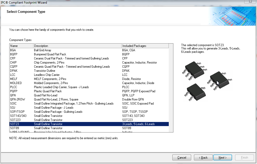
In the next window select SOT23
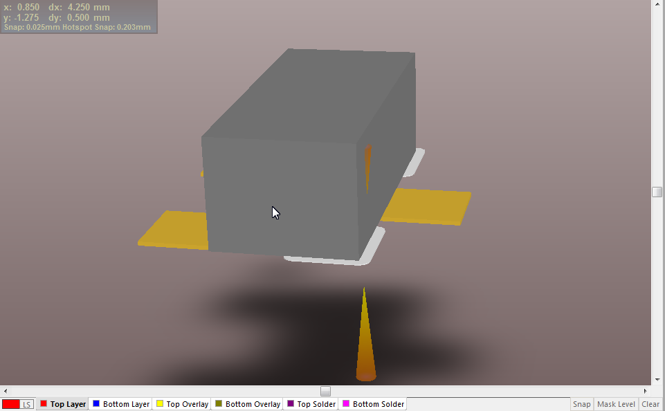
Press 3 to go to the 3D view and the 3D view of this part looks like the one below-
So in this way we can create a SOT23 transistor footprint plus the body part with Altium designer IPC complaint wizard.
One can also create a footprint using the component wizard and add a 3D model instead of using IPC complaint wizard. See example of this process - Footprint and 3D body for Switch
Also see all other altium designer tutorials
The transistor for which we are going to create the footprint is the MMBT3904LT1G from ON Semiconductor. The picture below shows how it looks like-
If you download the datasheet of this component you will find the dimension of the body and the footprint. The picture below shows the dimension cut from the datasheet-
This engineering drawing has all the dimension we need.
Once you have opened your PCB Library component editor in Altium Designer, click on the IPC Complaint Footprint Wizard which is under the Tools in the toolbar.
The startup window looks like this-
In the next window select SOT23
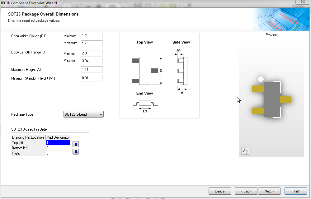
The next window is for entering the body dimension information. From the datasheet the dimension can be read and entered into the wizard.
The next window is for the Pin related dimension. This is also provided in the datasheet. Note that while entering here, the lead span range(E) in the wizard is the sum of the body width(E) in the datasheet and twice the length L1 in the datasheet.
The next window can be left in default as it automatically calculates the heel spacing and therefore is not shown here.
Next comes the solder fillets and the tolerances which can also be left in their default values.
The next major dimension we must be aware of is the footprint dimension. Altium automatically calculates the pad dimension but looking at the footprint in the datasheet they do not match. So we can change the setting here. This values entered are shown below-
Next comes the silk screen dimension which can also be left in their default values.
The body courtyard, aseembly and the component body information can also be left in their default values.
The next window is to provide name and description. Altium automatically inserts these information but one can change it.
The next thing is the where you want to save the footprint. Browse to the directory where you want to save it.
When you click Finish the footprint drawing looks like this-
One can also create a footprint using the component wizard and add a 3D model instead of using IPC complaint wizard. See example of this process - Footprint and 3D body for Switch
Also see all other altium designer tutorials


No comments:
Post a Comment