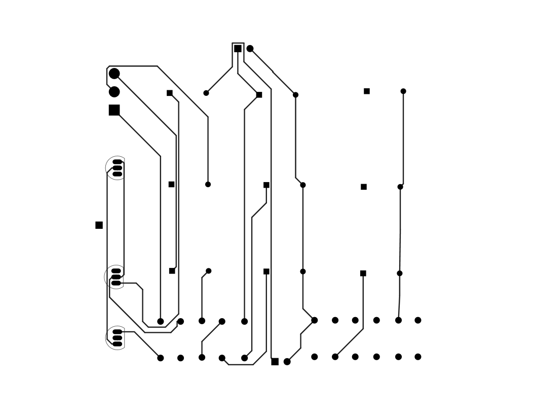
Once a PCB is designed an accurate drawing of the PCB layout can be produced called the Artwork. The Artwork can also be scaled up or down while retaining the dimension. It can also be used to create the PCB pattern using photography process. The Artwork drawing shows drawing of the copper traces, the solder pads and any conducting parts, their location, dimension and clearances to be imprinted on the board.
It is not the actual PCB file that is used for PCB manufacturing. It is the Gerber files, NC drill files etc are used for PCB board manufacturing. However for small scale design using manual PCB design process, the artwork can be used for PCB design. Artwork design are used to show design prototype and for analysis.

Artwork Scale is a term that refers to information about the scaled version of the artwork. It is indicated in terms of ratio which gives the relative accuracy of the artwork scale dimension over the PCB area. For example, one talks about artwork scale of 2:1 or 4:1. What artwork scale of 2:1 means is that the artwork drawing is 4 times that of the actual PCB area. The 4:1 artwork would give artwork 16 times the actual PCB area. Thus 4:1 is finer, more accurate and more detailed than the 2:1 artwork.
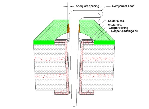
Artwork scale is useful in the manual PCB production. A manual layout design may require more precision and thus higher artwork scale. Added to this requirement is also the type of design. An integrated circuit with plated through holes also requires precise artwork scale for the PCB design.
It is not the actual PCB file that is used for PCB manufacturing. It is the Gerber files, NC drill files etc are used for PCB board manufacturing. However for small scale design using manual PCB design process, the artwork can be used for PCB design. Artwork design are used to show design prototype and for analysis.

Artwork Scale is a term that refers to information about the scaled version of the artwork. It is indicated in terms of ratio which gives the relative accuracy of the artwork scale dimension over the PCB area. For example, one talks about artwork scale of 2:1 or 4:1. What artwork scale of 2:1 means is that the artwork drawing is 4 times that of the actual PCB area. The 4:1 artwork would give artwork 16 times the actual PCB area. Thus 4:1 is finer, more accurate and more detailed than the 2:1 artwork.
Artwork scale is useful in the manual PCB production. A manual layout design may require more precision and thus higher artwork scale. Added to this requirement is also the type of design. An integrated circuit with plated through holes also requires precise artwork scale for the PCB design.


