A conceptual
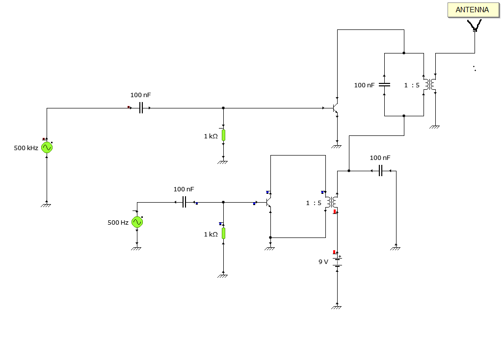
AM modulation circuit diagram is below. It is conceptual only because the values of the passive components are not real calculated values. That is it only shows a skeleton of a circuit that is supposed to do AM modulation. The transistors should be biased appropriately to make the circuit work. Look into transistor biasing tutorial.
In the circuit shown, the two signals, one 500Hz(within the frequency range of speech) and a 500KHz of the desired carrier signal is to be mixed and sent to the antenna.
 |
| Conceptual AM Modulation Circuit Diagram |
The audio signal is supposed to be amplified by a audio amplifier first. Then secondly the amplified audio signal is coupled by the lower transformer and enters the LC tank where the mixing takes place with the carrier signal. This process of audio signal flow in the circuit is shown by the picture below-
 |
| audio signal flow in am modulation circuit |
The upper part is a Tuned RF Amplifier-
 |
| tuned RF amplifier |
Now the carrier signal flow into the tuned RF circuit is shown below-
 |
| carrier signal flow in am circuit |
The mixing between the audio signal and the carrier signal takes place in the LC tank and the mixed signal ultimately passes into the antenna.
 |
| mixing of signal in am circuit |
This is how this AM circuit should work.
See other
AM circuit examples,
circuit and pcb examples


No comments:
Post a Comment