Thursday, August 13, 2026
Microphone Pre-Compressor Circuit for SSB Transceivers
Microphone Pre-Compressor Circuit for SSB Transceivers: A practical microphone pre-compressor circuit for SSB transceivers using JFET and transistor stages. Improve transmit audio clarity and power in amateur radio

Mini FM Radio Transmitter
Mini FM Radio Transmitter: FM Radio Transmitter takes your voice from a microphone and turns it into a r signal. Then, this radio signal can be picked up by any standard FM radio nearby.
Build Your Own 90MHz Crystal Controlled FM Transmitter
Build Your Own 90MHz Crystal Controlled FM Transmitter: A crystal controlled FM transmitter is a radio frequency circuit that uses quartz crystal oscillator to generate a stable, precise frequency for FM transmission
Tuesday, May 12, 2026
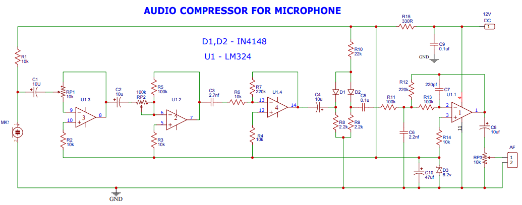
Audio compressor for microphone
This circuit diagram illustrates an audio compressor for microphone signals. Its primary job is to even out the volume of your voice, making soft sounds louder and loud sounds quieter, resulting in a more consistent and professional audio output. This is incredibly useful for podcasts, voice overs, amateur radio, or any application where microphone levels can fluctuate.
Monday, April 27, 2026
Microphone Preamplifier with Audio Peak Limiter
Microphone Preamplifier with Audio Peak Limiter: Build a simple microphone preamplifier with audio limiter using 2N3904 transistors and 1N34 diodes. Ideal for ham radio, DIY audio, or voice processing
Wednesday, July 23, 2025
Simple DIY Active Antenna for Crystal-Clear Reception
Simple DIY Active Antenna for Crystal-Clear Reception
Tired of static on your AM or shortwave radio? Do you struggle to hear distant stations? There is a simple fix. You can build a special antenna that makes radio signals much stronger. This guide shows you how to build a DIY active antenna. It is a fun project that can give you crystal-clear reception.
https://vu3dxr.in/simple-diy-active-antenna-for-crystal-clear-reception/
Tired of static on your AM or shortwave radio? Do you struggle to hear distant stations? There is a simple fix. You can build a special antenna that makes radio signals much stronger. This guide shows you how to build a DIY active antenna. It is a fun project that can give you crystal-clear reception.
https://vu3dxr.in/simple-diy-active-antenna-for-crystal-clear-reception/
Active Antenna and Signal Grabber Circuits for Enhanced Shortwave Reception
Active Antenna and Signal Grabber Circuits for Enhanced Shortwave Reception
Introduction to Active Antennas for Shortwave Receivers
In the world of shortwave listening (SWL), achieving optimal reception quality is paramount for radio enthusiasts and ham radio operators. Active antenna circuits and signal grabber designs have revolutionized how we approach shortwave reception, offering significant advantages over traditional passive antenna systems. These innovative solutions provide superior performance, especially in urban environments where space constraints and RF noise present ongoing challenges.
The concept of active antenna amplification involves integrating low-noise amplifiers directly into the antenna system, creating what some engineers call "antennafiers." This approach transforms short, compact antennas into high-performance receiving systems that can rival much larger installations.
Understanding Signal Grabber Circuits for Shortwave Reception
A simple signal grabber circuit for shortwave reception represents one of the most effective approaches to improving RF performance with minimal hardware requirements. These circuits typically employ a two-transistor design that provides critical impedance matching between short antennas and receiver inputs.
The fundamental principle behind signal grabber operation involves using high input impedance components to efficiently capture RF signals from short antennas, then providing low output impedance for optimal receiver matching. The circuit utilizes transistor Q1 with high input impedance and excellent high-frequency characteristics, making it ideal for short antenna applications. Meanwhile, Q2 provides low output impedance, creating a close match for typical receiver inputs.
Key Components in Signal Grabber Design
Modern signal grabber circuits incorporate specific active components optimized for shortwave performance:
- Q1 (MPF102): A general-purpose N-channel JFET that provides high input impedance
- Q2 (2N3904): A general-purpose NPN silicon transistor for impedance matching
- Supporting passive components for bias and filtering
The signal grabber operates on a simple but highly effective principle. The short antenna picks up RF signals and feeds them to Q1's high-impedance input, where Q1 amplifies the signal while maintaining excellent noise performance.
DIY Active Antenna Solutions for Crystal-Clear Reception
Building a simple DIY active antenna for crystal-clear reception offers shortwave enthusiasts an economical path to dramatically improved reception quality. These active antenna designs perform exceptionally well on shortwave bands, delivering performance comparable to a 20 to 30-foot wire antenna while occupying a fraction of the space.
Advantages of Active Antenna Systems
Active antenna circuits provide several compelling advantages over passive alternatives:
- Space Efficiency: Compact designs suitable for apartment dwellers and portable operations
- Noise Performance: Superior signal-to-noise ratios in urban RF environments
- Impedance Matching: Optimal interface between antenna elements and receiver inputs
- Gain Control: Adjustable amplification to prevent receiver overload
- Broadband Response: Effective across multiple shortwave bands
Technical Principles of Active Antenna Design
The effectiveness of active antenna amplifiers stems from their ability to address fundamental limitations of short antenna systems. Traditional short antennas suffer from poor radiation resistance and high reactance, resulting in inefficient signal capture and poor impedance matching to 50-ohm receiver inputs.
Active antenna circuits solve these problems by:
- Providing high input impedance to efficiently couple with short antenna elements
- Incorporating low-noise amplification to improve weak signal reception
- Delivering proper impedance transformation for optimal receiver matching
- Implementing gain control to prevent strong signal overload
Frequency Response and Band Coverage
Modern shortwave active antenna designs typically provide excellent performance across the entire HF spectrum, from 3 MHz to 30 MHz. This broad frequency response makes them ideal for:
- International broadcast reception
- Ham radio monitoring
- Utility station listening
- Time signal reception
- Maritime and aeronautical communications
Circuit Implementations and Design Variations
The circuits section at VU3DXR offers extensive resources for understanding various active antenna implementations. These range from simple two-transistor designs to more sophisticated differential amplifier configurations.
Magnetic Loop Active Antennas
Magnetic loop antennas combined with active amplifiers represent another popular approach for shortwave signal enhancement. These systems, sometimes called "hula-loop" antennas, offer excellent directional characteristics and superior noise rejection in urban environments.
The differential amplifier configuration commonly used in magnetic loop systems provides:
- Excellent common-mode noise rejection
- Balanced input characteristics
- Superior out-of-band signal rejection
- Varactor tuning capability for frequency selectivity
Practical Construction and Implementation
Building effective signal grabber circuits requires attention to several critical design factors:
Component Selection
Choosing appropriate active devices is crucial for optimal performance. JFETs like the MPF102 provide excellent high-frequency characteristics and low noise performance, while bipolar transistors like the 2N3904 offer reliable impedance transformation capabilities.
Power Supply Considerations
Active antenna amplifiers typically operate from low-voltage DC supplies, making them suitable for battery-powered portable operations. Most designs function effectively with supply voltages ranging from 9V to 15V, drawing minimal current for extended battery life.
RF Shielding and Grounding
Proper shielding and grounding practices are essential for preventing oscillation and maintaining stability in active antenna circuits. This includes using appropriate enclosures, implementing star grounding techniques, and ensuring adequate isolation between input and output circuits.
Performance Optimization and Troubleshooting
Maximizing the effectiveness of shortwave active antennas requires understanding common performance limitations and optimization techniques:
Gain Adjustment
Most active antenna designs incorporate gain control mechanisms to prevent receiver overload while maintaining adequate sensitivity for weak signals. This balance is crucial for optimal performance across varying signal conditions.
Bandwidth Considerations
While broadband response is generally desirable, some applications benefit from frequency-selective designs that provide enhanced rejection of out-of-band interference. This is particularly important in urban environments with high RF noise levels.
Integration with Modern Receivers
Contemporary shortwave receivers and SDR systems benefit significantly from properly designed active antenna interfaces. The impedance matching and signal conditioning provided by these circuits ensure optimal receiver performance while preventing overload conditions.
SDR Compatibility
Software-defined radio systems are particularly sensitive to proper signal conditioning, making active antenna amplifiers essential components for serious SDR-based shortwave listening stations.
Advanced Design Concepts
Modern active antenna technology continues to evolve, incorporating advanced concepts like:
- Digitally controlled gain adjustment
- Frequency-specific optimization
- Adaptive noise cancellation
- Remote control capabilities
- Integration with antenna switching systems
Circuit Resources and Further Development
The comprehensive circuit collection available at VU3DXR provides extensive resources for shortwave enthusiasts interested in building and optimizing active antenna systems. These resources include detailed schematics, construction notes, and performance measurements for various designs.
Additional circuit resources cover related topics including:
- HF antenna designs for specific band requirements
- QRP transmitter circuits for two-way communication
- RF amplifier designs for various applications
Conclusion
Active antenna circuits and signal grabber designs represent essential tools for serious shortwave listeners and ham radio operators. These systems provide dramatic performance improvements while addressing the practical constraints of space-limited installations and urban RF environments.
The combination of proper circuit design, quality components, and careful construction techniques enables compact active antenna systems to deliver performance rivaling much larger passive installations. For shortwave enthusiasts seeking to maximize their reception capabilities, investing time in understanding and implementing these technologies pays substantial dividends in improved reception quality and listening satisfaction.
Whether building a simple two-transistor signal grabber or implementing a sophisticated magnetic loop system with differential amplification, the principles and resources outlined here provide the foundation for successful shortwave active antenna projects. The continued evolution of these technologies ensures that space-constrained operators can enjoy world-class shortwave reception performance regardless of their installation limitations.
For more detailed circuit diagrams, construction articles, and technical resources, visit the comprehensive electronics library at VU3DXR.in, featuring extensive coverage of ham radio projects, antenna designs, and RF circuit implementations.
Friday, July 18, 2025
Terminated End Fed Antenna: Complete Technical Guide for Ham Radio Operations
Terminated End Fed Antenna: Complete Technical Guide for Ham Radio Operations
Introduction
The terminated end fed antenna represents one of the most versatile and efficient antenna designs for modern amateur radio operations. Unlike traditional end fed antennas that exhibit standing wave patterns, terminated end fed antennas utilize a termination resistor to create a traveling wave antenna system. This comprehensive guide explores the technical aspects, design considerations, and practical implementation of terminated end fed antennas, with detailed circuit analysis and construction techniques.
What is a Terminated End Fed Antenna?
A terminated end fed antenna is a traveling wave antenna system where the antenna has a constant current distribution along its length. The key distinguishing feature is the termination resistor at the far end of the antenna, which absorbs the energy that would otherwise be reflected back toward the feed point.
The most popular variant is the Terminated End Fed Vee Antenna (TEFV), which offers exceptional multiband performance with minimal SWR across a wide frequency range. This design has gained significant popularity among amateur radio operators due to its simplicity and effectiveness.
Technical Principles and Theory
Traveling Wave Operation
The fundamental principle behind terminated end fed antennas lies in their traveling wave operation. When properly terminated, the antenna eliminates standing waves by absorbing the energy that reaches the far end. This results in:
- Constant current distribution along the antenna length
- Unidirectional radiation pattern toward the terminated end
- Broadband operation without the need for complex matching networks
- Reduced ground losses compared to traditional antenna systems
Termination Resistor Requirements
The termination resistor is critical to the antenna's performance. Values between 300-600 ohms are common, with 450 ohms being typical for many installations. The exact value depends on several factors:
- Antenna geometry and configuration
- Height above ground
- Desired frequency response
- Power handling requirements
The resistor should be rated to safely absorb at least 1/3 of the applied transmitter power for SSB operation, with higher ratings recommended for continuous modes.
Design Variants and Configurations
Terminated End Fed Vee Antenna (TEFV)
The TEFV antenna design represents the most popular implementation of terminated end fed principles. This configuration offers:
- Multiband operation from 1.8 to 30 MHz
- Low SWR across the entire HF spectrum
- Simple construction with minimal components
- Excellent DX performance
T2FD (Tilted Terminated Folded Dipole)
The T2FD antenna is another excellent example of terminated antenna design. This provides an acceptable all-frequency match to commonly available 75 Ω coaxial cable and is terminated with a 400-480 Ω non-inductive resistor.
For detailed information about various terminated antenna configurations, visit the comprehensive guide on Terminated Antennas for HF Ham Radio.
Circuit Design and Matching Networks
Impedance Transformation
Most terminated end fed antennas require an impedance transformation network at the feed point. The most common approach uses a 9:1 current balun to transform the 50-ohm coaxial cable impedance to approximately 450 ohms at the antenna feed point.
Termination Circuit Design
The termination circuit typically consists of:
- Non-inductive resistor (typically 400-500 ohms)
- Heat sink assembly for power dissipation
- Weather protection enclosure
- Ground connection (for some configurations)
The resistor value should be 10% higher than the transformer output impedance. So for a 9:1 transformer (50 ohms to 450 ohms) the termination should be 500 ohms.
Construction Techniques and Best Practices
Wire Selection and Length
For optimal performance, the antenna wire should be:
- Stranded copper for flexibility and conductivity
- 14 AWG minimum for power handling capability
- Length optimized for the desired frequency range
Termination Resistor Installation
If you're building a terminated end-fed antenna, ensure the resistor is securely mounted and properly heatsinked if necessary, especially for higher power levels. Key considerations include:
- Proper heat sinking for power dissipation
- Weather protection to prevent corrosion
- Secure mounting to prevent mechanical stress
- Low-inductance construction to maintain broadband performance
Grounding Considerations
Some terminated antenna designs benefit from proper grounding at the termination point. A 9:1 current balun was used at the feed point with a single 1m ground rod as the earth connection. At the far end a 390 ohm 50W rated thick film resistor was mounted in a diecast aluminium box as heatsink and connected to another 1m ground rod.
Performance Characteristics
Radiation Pattern
Terminated end fed antennas exhibit unidirectional radiation patterns with the main lobe directed toward the terminated end. By terminating the remote end it means that one end is terminated by the load, i.e. transmitter or receiver, and the remote end is terminated by the resistor.
Frequency Response
The broadband nature of terminated antennas makes them ideal for:
- Contest operations requiring quick band changes
- Digital modes with varying frequency requirements
- Emergency communications where versatility is crucial
- Portable operations where antenna space is limited
Practical Applications
Field Expedient Installations
Terminated end fed antennas excel in portable applications due to their:
- Simple deployment requirements
- Minimal ground system needs
- Multiband capability without tuning
- Compact termination hardware
Fixed Station Applications
For permanent installations, terminated antennas offer:
- Consistent performance across all bands
- Reduced maintenance compared to complex arrays
- Space-efficient design for restricted locations
- Excellent DX capabilities
Troubleshooting and Optimization
Common Issues and Solutions
- High SWR: Check termination resistor value and connections
- Poor DX performance: Verify antenna orientation and height
- Resistor overheating: Increase power rating or improve heat sinking
- Pattern distortion: Check for nearby metallic objects
Performance Optimization
To maximize antenna performance:
- Optimize antenna height for desired coverage
- Use quality termination resistors with proper power ratings
- Implement proper balun design for impedance matching
- Minimize common mode currents with effective choking
Advanced Designs and Modifications
Rhombic Antenna Termination
For specialized applications, 600 to 800 ohm non-inductive resistors to terminate the antennas, making rhombic rhombic directional with FB of more than 30 db on these long antennas provide exceptional directivity.
Custom Termination Networks
Advanced builders can explore custom termination networks for specific applications, incorporating:
- Frequency-dependent termination for optimized performance
- Reactive termination for enhanced bandwidth
- Switched termination for pattern control
Conclusion
Terminated end fed antennas represent an excellent choice for amateur radio operators seeking versatile, high-performance antenna systems. The combination of broadband operation, simple construction, and excellent DX capabilities makes them ideal for both portable and fixed station applications.
The TEFV antenna design and other terminated antenna configurations offer proven performance across the HF spectrum. By understanding the technical principles and following proper construction techniques, amateur radio operators can build highly effective antenna systems that serve them well for years to come.
For additional technical resources and detailed construction guides, visit VU3DXR.in for comprehensive antenna design information and circuit analysis.
AM Radio Transmitter Circuits for Beginners: A Step-by-Step Guide
AM Radio Transmitter Circuits for Beginners: A Step-by-Step Guide
Building an AM radio transmitter is an exciting project for electronics enthusiasts, especially beginners eager to explore radio frequency (RF) circuits. Amplitude Modulation (AM) transmitters are ideal for learning due to their simplicity and accessible components. In this SEO-optimized article, we’ll dive into beginner-friendly AM transmitter circuits from the vu3dxr.in blog, with direct links to their detailed schematics. We’ll also include external resources for authenticity and tips to boost your project’s success, all while driving backlinks to vu3dxr.in.
Why Build an AM Radio Transmitter?
AM transmitters modulate the amplitude of a carrier wave to transmit audio, operating in the medium wave band (500kHz–1600kHz). They’re simpler than FM circuits, making them perfect for hands-on learning about oscillators, modulation, and RF design. With circuits from vu3dxr.in, you can broadcast audio to a nearby AM radio and gain practical electronics experience.
Note: Transmitting without a license is illegal in most countries. Always check local regulations, such as FCC Part 15 rules, before testing. These circuits are for educational purposes.
Key Components of an AM Transmitter
A basic AM transmitter includes:
- Audio Amplifier: Boosts the audio input (e.g., from a microphone).
- RF Oscillator: Generates the carrier wave.
- Modulator: Combines audio with the carrier.
- Tank Circuit: Tunes the frequency using an inductor (L) and capacitor (C).
- Antenna: Radiates the signal.
You can source components like transistors (e.g., 2N3904) and capacitors from suppliers like DigiKey or salvage them from old radios, as suggested on vu3dxr.in’s Homebrew RF Circuits page.
Beginner-Friendly AM Transmitter Circuit from vu3dxr.in
The Series Modulated AM Transmitter from vu3dxr.in is a fantastic starting point for beginners. This low-power, crystal-controlled circuit is perfect for QRP (low-power) projects and uses minimal components.
Circuit Overview
- Crystal Oscillator: Ensures stable frequency output (e.g., 1000kHz).
- Transistor Q5: Modulates the carrier by varying the power supply.
- Potentiometer VR1 (10k): Adjusts Q5’s collector voltage to 6.6V.
- Tank Circuit (L1, C1): Tunes the signal to the desired frequency.
Link: Series Modulated AM Transmitter on vu3dxr.in
How It Works
- The crystal oscillator generates a stable carrier wave.
- Audio input (e.g., from a microphone) modulates the power supply via Q5.
- The tank circuit filters the signal to the AM band.
- A 10-foot wire antenna radiates the signal, receivable on a nearby AM radio.
Building Tips
- Use a crystal matching your target frequency (e.g., 1000kHz).
- Adjust VR1 for clear audio output.
- Match the antenna impedance with L2 and C2, as detailed in vu3dxr.in’s guide.
A Simpler Alternative: Poor-Man’s Transmitter
For an even easier build, try the Poor-Man’s Transmitter from vu3dxr.in. This circuit is ideal for creating a simple AM radio beacon using vintage components.
Circuit Highlights
- Oscillator: A single 2N3904 transistor generates the carrier.
- Modulation: A condenser microphone provides audio input.
- Tank Circuit: A variable capacitor (300–500pF) and inductor allow manual tuning.
- Power: Runs on a 9V battery.
Link: Poor-Man’s Transmitter on vu3dxr.in
Construction Steps
- Build the oscillator with a 2N3904 and LC tank circuit.
- Connect a condenser microphone for modulation.
- Power with a 9V battery and attach a 3–10-foot antenna.
- Tune the variable capacitor to your desired AM frequency.
Why It’s Great for Beginners
- Minimal components simplify assembly.
- Manual tuning teaches tank circuit fundamentals.
- Portable and low-cost, using salvaged parts.
Learn More: Homebrew RF Circuits on vu3dxr.in for component sourcing tips.
Common Beginner Questions
How Do I Tune the Frequency?
The Poor-Man’s Transmitter uses a variable capacitor for manual tuning. For fixed frequencies, the Series Modulated AM Transmitter relies on a crystal.
Can I Increase the Range?
Optimize the antenna and impedance matching, as explained in vu3dxr.in’s Homebrew RF Circuits. A 10–15-foot wire antenna can extend range within legal limits.
What If I Want a Beacon Without Audio?
Remove the microphone from either circuit. For the Series Modulated AM Transmitter, adjust VR1 for a steady carrier signal.
Where to Get Components?
Salvage from old radios or buy from Mouser Electronics. Vu3dxr.in’s Homebrew RF Circuits suggests local markets for vintage parts.
Safety and Legal Notes
- Low Power: Stay within legal limits (e.g., FCC Part 15).
- Licensing: Obtain a ham radio license for legal operation. Visit ARRL for details.
- Interference: Use proper filtering, as outlined in the Series Modulated AM Transmitter.
Why vu3dxr.in Is Your Go-To Resource
The vu3dxr.in blog offers:
- Detailed schematics for the Series Modulated AM Transmitter and Poor-Man’s Transmitter.
- Practical advice on QRP and DIY RF projects.
- Tips for troubleshooting and component sourcing via Homebrew RF Circuits.
Conclusion
Building an AM radio transmitter is a rewarding way to learn RF electronics. The Series Modulated AM Transmitter and Poor-Man’s Transmitter from vu3dxr.in are perfect for beginners. With minimal components and clear instructions, you can broadcast audio to a nearby AM radio. Explore more DIY RF projects at vu3dxr.in’s Homebrew RF Circuits and check Circuit Basics for additional tutorials. Always follow local regulations to enjoy this hobby safely.
Tuesday, July 15, 2025
ATS Mini DSP Radio Floods the Market: What's Behind the Surge?
ATS Mini DSP Radio Floods the Market: What's Behind the Surge?
The ATS Mini DSP Radio has been making waves in the radio enthusiast community, with a recent surge in demand leading to a flood of devices hitting the market. According to reports from VU3DXR's blog, the device has been selling out quickly, with many enthusiasts and professionals alike clamoring to get their hands on the compact, feature-rich SDR.
The ATS Mini DSP Radio's popularity can be attributed to its impressive technical specifications and versatility. As detailed in VU3DXR's technical analysis, the device boasts a robust architecture and advanced DSP capabilities, making it an attractive option for those looking to upgrade their radio setup.
The sudden increase in demand has led to a surge in availability, with many retailers and online marketplaces now stocking the device. For those looking to purchase an ATS Mini DSP Radio, VU3DXR's buying guide provides valuable insights and tips on how to navigate the market.
As the ATS Mini DSP Radio continues to gain popularity, it's clear that its impact is being felt across the radio enthusiast community. For the latest updates and news on the device, stay tuned to VU3DXR's blog, which is providing in-depth coverage of the ATS Mini DSP Radio phenomenon.
Thursday, July 17, 2014
What is Artwork and Artwork Scale in PCB Design?
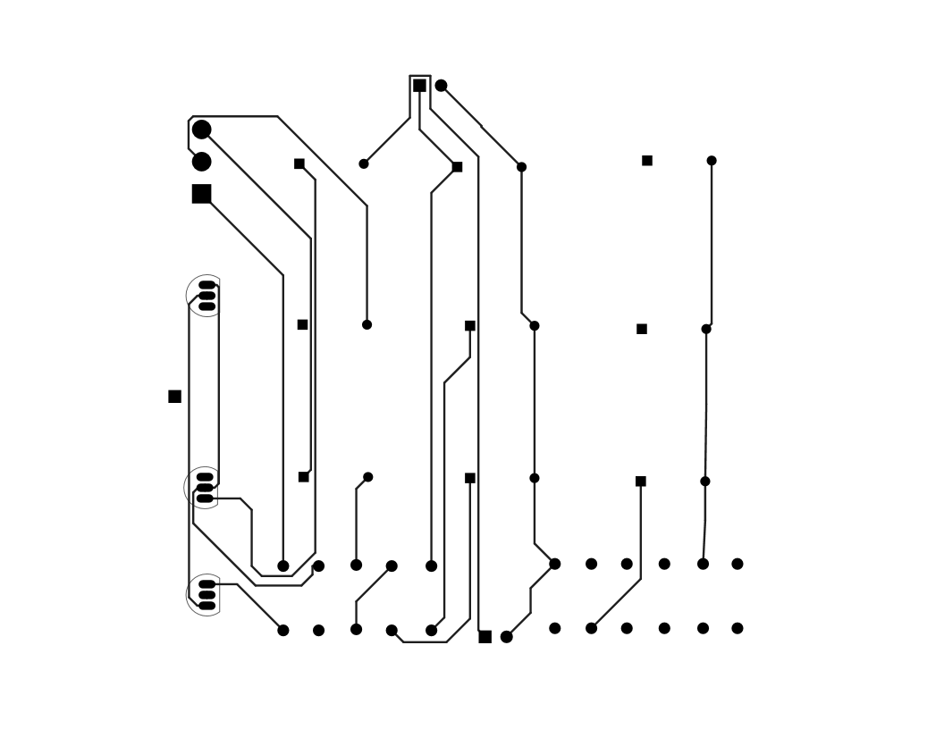
Once a PCB is designed an accurate drawing of the PCB layout can be produced called the Artwork. The Artwork can also be scaled up or down while retaining the dimension. It can also be used to create the PCB pattern using photography process. The Artwork drawing shows drawing of the copper traces, the solder pads and any conducting parts, their location, dimension and clearances to be imprinted on the board.
It is not the actual PCB file that is used for PCB manufacturing. It is the Gerber files, NC drill files etc are used for PCB board manufacturing. However for small scale design using manual PCB design process, the artwork can be used for PCB design. Artwork design are used to show design prototype and for analysis.

Artwork Scale is a term that refers to information about the scaled version of the artwork. It is indicated in terms of ratio which gives the relative accuracy of the artwork scale dimension over the PCB area. For example, one talks about artwork scale of 2:1 or 4:1. What artwork scale of 2:1 means is that the artwork drawing is 4 times that of the actual PCB area. The 4:1 artwork would give artwork 16 times the actual PCB area. Thus 4:1 is finer, more accurate and more detailed than the 2:1 artwork.
Artwork scale is useful in the manual PCB production. A manual layout design may require more precision and thus higher artwork scale. Added to this requirement is also the type of design. An integrated circuit with plated through holes also requires precise artwork scale for the PCB design.
It is not the actual PCB file that is used for PCB manufacturing. It is the Gerber files, NC drill files etc are used for PCB board manufacturing. However for small scale design using manual PCB design process, the artwork can be used for PCB design. Artwork design are used to show design prototype and for analysis.
Artwork Scale is a term that refers to information about the scaled version of the artwork. It is indicated in terms of ratio which gives the relative accuracy of the artwork scale dimension over the PCB area. For example, one talks about artwork scale of 2:1 or 4:1. What artwork scale of 2:1 means is that the artwork drawing is 4 times that of the actual PCB area. The 4:1 artwork would give artwork 16 times the actual PCB area. Thus 4:1 is finer, more accurate and more detailed than the 2:1 artwork.
Artwork scale is useful in the manual PCB production. A manual layout design may require more precision and thus higher artwork scale. Added to this requirement is also the type of design. An integrated circuit with plated through holes also requires precise artwork scale for the PCB design.
Wednesday, July 16, 2014
How to select a good PCB design software?
PCB design automation is essential in today's market competition. Even if it is not for selling design design professional want to know the best PCB design software for research for example. While small design can be completed with open source software, larger and complex design requires high accuracy, high performance software. In the PCB design process routing is perhaps the critical part that designers constantly focus on. Many PCB has auto router feature but often it does the provide the optimum path. And what is design automation if this part of work cannot be automated? Modern PCB software does take great deal of work load from the designer.
So how to select a good PCB design software?
Most of the PCB design software provides schematic design, simulation, PCB design, auto routing features.
A typical PCB CAD software vendor offers demo. The demo software has demo license and one should use it to exploit its strength and weakness. Once you have the demo software, you should look into couple of things as follows.

Check the demo board but don't rely on that. Instead think of it as the best you can get from the software if the software really functions are advertized. Because the vendor always would, should and do provide their best PCB design to demonstrate the software capability.
Now what really matters and the things one should watch in the application is the Auto Routing program, the EMI and thermal technological support and restrictions, the accuracy of the wire frames, the units accuracy, the number of PCB layers it can support, the export to other CAD software, the CAM support. Another important selection criteria is the library support, the parts and documentation, how footprints have to be created, the simulation capability for the parts.
You don't want to spend time on debugging your design once you buy the PCB CAD. You want to have the PCB CAD automate most of the design work with high accuracy as much as possible.
See schematic and PCB design tutorials
So how to select a good PCB design software?
Most of the PCB design software provides schematic design, simulation, PCB design, auto routing features.
A typical PCB CAD software vendor offers demo. The demo software has demo license and one should use it to exploit its strength and weakness. Once you have the demo software, you should look into couple of things as follows.
Check the demo board but don't rely on that. Instead think of it as the best you can get from the software if the software really functions are advertized. Because the vendor always would, should and do provide their best PCB design to demonstrate the software capability.
Now what really matters and the things one should watch in the application is the Auto Routing program, the EMI and thermal technological support and restrictions, the accuracy of the wire frames, the units accuracy, the number of PCB layers it can support, the export to other CAD software, the CAM support. Another important selection criteria is the library support, the parts and documentation, how footprints have to be created, the simulation capability for the parts.
You don't want to spend time on debugging your design once you buy the PCB CAD. You want to have the PCB CAD automate most of the design work with high accuracy as much as possible.
See schematic and PCB design tutorials
Open Source Virtual Electronics breadboard Software
Fritzing is an open source Virtual Electronics design with virtual breadboard software. It is an interesting software because the look of the PCB and schematic looks very realistic. The components looks very realistic which makes it easy to understand and imagine the final design. The components can be dragged into the virtual breadboard and together they look very realistic. It is also a schematic drawing software which means schematic of the electronics circuit can be drawn easily and transferred to the PCB. Components if not available can be created with the component editor quickly.
A view of virtual breadboard and printed circuit board where components are placed is shown for illustration.

This virtual electronics design software is useful for students, beginners and electronics hobbyist and for teaching purpose. The realistic view of the design makes it easy to learn schematic and PCB design. Following shows a picture of parts which looks very nice and realistic.

Also various kinds and size of project can be completed with Fritzing such Arduino microcontroller project, RF project, robotics and others. A large number of schematic and pcb design tutorials are provided in the Fritzing website which makes it even more easier for people to learn designing with the software.
A view of virtual breadboard and printed circuit board where components are placed is shown for illustration.

This virtual electronics design software is useful for students, beginners and electronics hobbyist and for teaching purpose. The realistic view of the design makes it easy to learn schematic and PCB design. Following shows a picture of parts which looks very nice and realistic.

Also various kinds and size of project can be completed with Fritzing such Arduino microcontroller project, RF project, robotics and others. A large number of schematic and pcb design tutorials are provided in the Fritzing website which makes it even more easier for people to learn designing with the software.
How to start and configure web application developement with Matlab
Matlab has a feature to create web application. For people who are trying this feature for the first time to make the feature work can be quite confusing. How this matlab web application development feature works is that the Matlab code are converted to java code(java class strickly speaking) by Matlab Builder JA. Malab Builder JA is smaller and essential part for the conversion. The overall conversion of matlab code to web is through the Java application package creation which contains java components of all matlab code of your project and required components. Java package is created using the Library Compiler.
In order to use Matlab for web application deployment you need Java Development Kit(JDK). So the first thing to do is find the compatible version of the JDK that you have to download and install for your computer.
Enter the following matlab command to know which version of JDK you need,
!java- version
In matlab command window it looks like this if you did install version 1.7,
>> !java -version
java version "1.7.0_55"
Java(TM) SE Runtime Environment (build 1.7.0_55-b14)
Java HotSpot(TM) Client VM (build 24.55-b03, mixed mode, sharing)
Once you know this you should download that version of JDK.
Alternatively, you can also visit the following matlab page where you can see what version of different compilers and third party tools you requires according to the Matlab version you are using.
Assuming that you are using Matlab 2014a then the following url provides the information about the JDK version you need.
The figure shows that Matlab 2014a requires Java Development Kit(JDK) 1.7. So go to the Java website and download it. On the Java website it is listed as Java v7 which might cause confusion because it means the JDK v1.7.
Once you have download and installed the correct JDK you need to next set the JAVA_HOME environment variable path to the directory where you installed the JDK,something like C:\Program Files\Java\jdk1.7.0_65 so that Matlab knows and applies the java function. If this is not set then during the java package compilation you may get error.
Assuming you know how to set system environment variable, below is a screenshot of how it looks like,
That it, now you should be able to convert the matlab m code or GUI to Java Package using the Library Compiler. the Libary compiler is shown below. In the library compiler you select the Java Package in the application type and also select the matlab file to be exported.
The process of conversion produces three folders as follows,
for_redistribution — A folder containing the installer to distribute the package
for_testing — A folder containing the raw generated files to create the installer
for_redistribution_files_only — A folder containing only the files needed to redistribute the package
PackagingLog.txt — A log file generated by the compiler
Then one can check whether the produced java application is successful using the following command in the matlab command window,
java -classpath "matlabroot\toolbox\javabuilder\jar\javabuilder.jar";<file_name>.jar <file-name>.Class1 5
See matlab tutorials page for more tutorials
In order to use Matlab for web application deployment you need Java Development Kit(JDK). So the first thing to do is find the compatible version of the JDK that you have to download and install for your computer.
Enter the following matlab command to know which version of JDK you need,
!java- version
In matlab command window it looks like this if you did install version 1.7,
>> !java -version
java version "1.7.0_55"
Java(TM) SE Runtime Environment (build 1.7.0_55-b14)
Java HotSpot(TM) Client VM (build 24.55-b03, mixed mode, sharing)
Once you know this you should download that version of JDK.
Alternatively, you can also visit the following matlab page where you can see what version of different compilers and third party tools you requires according to the Matlab version you are using.
Assuming that you are using Matlab 2014a then the following url provides the information about the JDK version you need.
http://www.mathworks.com/support/compilers/R2014a/index.html
There you can see what Java JDK version you need as shown below
 |
| Choosing JDK version for matlab web developement |
The figure shows that Matlab 2014a requires Java Development Kit(JDK) 1.7. So go to the Java website and download it. On the Java website it is listed as Java v7 which might cause confusion because it means the JDK v1.7.
Once you have download and installed the correct JDK you need to next set the JAVA_HOME environment variable path to the directory where you installed the JDK,something like C:\Program Files\Java\jdk1.7.0_65 so that Matlab knows and applies the java function. If this is not set then during the java package compilation you may get error.
Assuming you know how to set system environment variable, below is a screenshot of how it looks like,
 |
| setting JAVA_HOME environmental variable |
That it, now you should be able to convert the matlab m code or GUI to Java Package using the Library Compiler. the Libary compiler is shown below. In the library compiler you select the Java Package in the application type and also select the matlab file to be exported.
 |
| Using Java Package Compiler in Matlab |
The process of conversion produces three folders as follows,
for_redistribution — A folder containing the installer to distribute the package
for_testing — A folder containing the raw generated files to create the installer
for_redistribution_files_only — A folder containing only the files needed to redistribute the package
PackagingLog.txt — A log file generated by the compiler
Then one can check whether the produced java application is successful using the following command in the matlab command window,
java -classpath "matlabroot\toolbox\javabuilder\jar\javabuilder.jar";<file_name>.jar <file-name>.Class1 5
See matlab tutorials page for more tutorials
Wireless Home theater Circuit using Bluetooth Headset
The post discusses a 200 + 200 watt wireless home theater circuit using a class D amplifier and a Bluetooth headset as the wireless module. The idea was requested by Mr. Sudipta Mandal.
The Request
The Request
I want to make my home theater wireless. My home theater model is Sony SRS-D9 2.1 channel. I also want the audio to be stereo. Range should me minimum 2 meters. Is it possible through Bluetooth module or RF transmitter & receiver? If so please suggest how to connect these modules to transmit and receive audio signals. If it is possible through Bluetooth then how to connect the Bluetooth module to my home theater? If a small circuit is required I can make it on my own but for that I need the circuit diagram and specifications of components required.
The Design
The Design
In one of the previous articles we learned regarding the internal constituents of a Bluetooth headset gadget and in another post we discussed how its speaker pins could be used for activating a relay.
In response to the above request, in this article we investigate how a Bluetooth Headset could be used for making a home theater system circuit.
The idea is simple, it's about finding a suitable differential power amplifier circuit and integrating the Bluetooth Headset speaker wires with the inputs of the amplifier.
For the proposed application here we have used an example 200 + 200 watt class D power amplifier circuit using the IC TDA8953 from NXP Semiconductors.
The complete schematic of the power amplifier can be witnessed in the below given diagram. It includes two differential inputs meaning the chip supports a stereo class D input.
The output is single ended though and is capable of driving two ground referenced 4 ohm speakers rated at 200+ watts each.

Each of the inputs of the above shown class D amplifier could be directly configured with the cut/stripped speaker wires of a scavenged Bluetooth headset circuit as given below:

Disconnect the speaker wires from the speaker, strips the ends carefully for the recommended integrations with the amplifier inputs

For using both the inputs of the amplifier and for enjoying a stereophonic home theater response, another compatible and appropriately paired Bluetooth headset unit will be required.
Once the integration of the two Headsets, paired with source Bluetooth is done, a throbbing crystal clear class D 400 watt stereo music could be experienced over the attached speakers.
The system could be positioned as a home theater system or simply for enjoying a pure 400 watts of music from your cell phone or other Bluetooth compatible gadgets.
If you already have a ready made home theater amplifier system, connect the input of the amplifier with any one cut/stripped speaker wire of the Bluetooth headset (if the amplifier is not a differential type) and make sure the negative line of the headset is made common with the amplifier negative line.
Alternatively a bridge network could be employed for rectifying the differential output from the headset speaker and the output could be directly joined with the inputs of the single ended amplifier.
Subscribe to:
Posts (Atom)